
Pinout Description :
Pins 1-8: Port 1 Each of these pins can be configured as an input or an output.
Pin 9: RS A logic one on this pin disables the microcontroller and clears the contents of most registers. In other words, the positive voltage on this pin resets the microcontroller. By applying logic zero to this pin, the program starts execution from the beginning.
Pins10-17: Port 3 Similar to port 1, each of these pins can serve as general input or output. Besides, all of them have alternative functions:
Pin 10: RXD Serial asynchronous communication input or Serial synchronous communication output.
Pin 11: TXD Serial asynchronous communication output or Serial synchronous communication clock output.
Pin 12: INT0 Interrupt 0 input.
Pin 13: INT1 Interrupt 1 input.
Pin 14: T0 Counter 0 clock input.
Pin 15: T1 Counter 1 clock input.
Pin 16: WR Write to external (additional) RAM.
Pin 17: RD Read from external RAM.
Pin 18, 19: X2, X1 Internal oscillator input and output. A quartz crystal which specifies operating frequency is usually connected to these pins. Instead of it, miniature ceramics resonators can also be used for frequency stability. Later versions of microcontrollers operate at a frequency of 0 Hz up to over 50 Hz.
Pin 20: GND Ground.
Pin 21-28: Port 2 If there is no intention to use external memory then these port pins are configured as general inputs/outputs. In case external memory is used, the higher address byte, i.e. addresses A8-A15 will appear on this port. Even though memory with capacity of 64Kb is not used, which means that not all eight port bits are used for its addressing, the rest of them are not available as inputs/outputs.
Pin 29: PSEN If external ROM is used for storing program then a logic zero (0) appears on it every time the microcontroller reads a byte from memory.
Pin 30: ALE Prior to reading from external memory, the microcontroller puts the lower address byte (A0-A7) on P0 and activates the ALE output. After receiving signal from the ALE pin, the external register (usually 74HCT373 or 74HCT375 add-on chip) memorizes the state of P0 and uses it as a memory chip address. Immediately after that, the ALU pin is returned its previous logic state and P0 is now used as a Data Bus. As seen, port data multiplexing is performed by means of only one additional (and cheap) integrated circuit. In other words, this port is used for both data and address transmission.
Pin 31: EA By applying logic zero to this pin, P2 and P3 are used for data and address transmission with no regard to whether there is internal memory or not. It means that even there is a program written to the microcontroller, it will not be executed. Instead, the program written to external ROM will be executed. By applying logic one to the EA pin, the microcontroller will use both memories, first internal then external (if exists).
Pin 32-39: Port 0 Similar to P2, if external memory is not used, these pins can be used as general inputs/outputs. Otherwise, P0 is configured as address output (A0-A7) when the ALE pin is driven high (1) or as data output (Data Bus) when the ALE pin is driven low (0).
Pin 40: VCC +5V power supply.
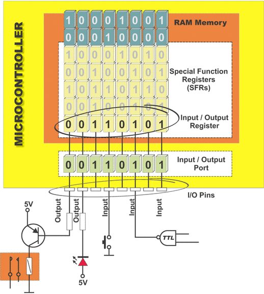
2.3 Input/Output Ports (I/O Ports) All 8051 microcontrollers have 4 I/O ports each comprising 8 bits which can be configured as inputs or outputs. Accordingly, in total of 32 input/output pins enabling the microcontroller to be connected to peripheral devices are available for use.
Pin configuration, i.e. whether it is to be configured as an input (1) or an output (0), depends on its logic state. In order to configure a microcontroller pin as an output, it is necessary to apply a logic zero (0) to appropriate I/O port bit. In this case, voltage level on appropriate pin will be 0.
Similarly, in order to configure a microcontroller pin as an input, it is necessary to apply a logic one (1) to appropriate port. In this case, voltage level on appropriate pin will be 5V (as is the case with any TTL input). This may seem confusing but don't loose your patience. It all becomes clear after studying simple electronic circuits connected to an I/O pin.
Pins 1-8: Port 1 Each of these pins can be configured as an input or an output.
Pin 9: RS A logic one on this pin disables the microcontroller and clears the contents of most registers. In other words, the positive voltage on this pin resets the microcontroller. By applying logic zero to this pin, the program starts execution from the beginning.
Pins10-17: Port 3 Similar to port 1, each of these pins can serve as general input or output. Besides, all of them have alternative functions:
Pin 10: RXD Serial asynchronous communication input or Serial synchronous communication output.
Pin 11: TXD Serial asynchronous communication output or Serial synchronous communication clock output.
Pin 12: INT0 Interrupt 0 input.
Pin 13: INT1 Interrupt 1 input.
Pin 14: T0 Counter 0 clock input.
Pin 15: T1 Counter 1 clock input.
Pin 16: WR Write to external (additional) RAM.
Pin 17: RD Read from external RAM.
Pin 18, 19: X2, X1 Internal oscillator input and output. A quartz crystal which specifies operating frequency is usually connected to these pins. Instead of it, miniature ceramics resonators can also be used for frequency stability. Later versions of microcontrollers operate at a frequency of 0 Hz up to over 50 Hz.
Pin 20: GND Ground.
Pin 21-28: Port 2 If there is no intention to use external memory then these port pins are configured as general inputs/outputs. In case external memory is used, the higher address byte, i.e. addresses A8-A15 will appear on this port. Even though memory with capacity of 64Kb is not used, which means that not all eight port bits are used for its addressing, the rest of them are not available as inputs/outputs.
Pin 29: PSEN If external ROM is used for storing program then a logic zero (0) appears on it every time the microcontroller reads a byte from memory.
Pin 30: ALE Prior to reading from external memory, the microcontroller puts the lower address byte (A0-A7) on P0 and activates the ALE output. After receiving signal from the ALE pin, the external register (usually 74HCT373 or 74HCT375 add-on chip) memorizes the state of P0 and uses it as a memory chip address. Immediately after that, the ALU pin is returned its previous logic state and P0 is now used as a Data Bus. As seen, port data multiplexing is performed by means of only one additional (and cheap) integrated circuit. In other words, this port is used for both data and address transmission.
Pin 31: EA By applying logic zero to this pin, P2 and P3 are used for data and address transmission with no regard to whether there is internal memory or not. It means that even there is a program written to the microcontroller, it will not be executed. Instead, the program written to external ROM will be executed. By applying logic one to the EA pin, the microcontroller will use both memories, first internal then external (if exists).
Pin 32-39: Port 0 Similar to P2, if external memory is not used, these pins can be used as general inputs/outputs. Otherwise, P0 is configured as address output (A0-A7) when the ALE pin is driven high (1) or as data output (Data Bus) when the ALE pin is driven low (0).
Pin 40: VCC +5V power supply.
2.3 Input/Output Ports (I/O Ports) All 8051 microcontrollers have 4 I/O ports each comprising 8 bits which can be configured as inputs or outputs. Accordingly, in total of 32 input/output pins enabling the microcontroller to be connected to peripheral devices are available for use.
Pin configuration, i.e. whether it is to be configured as an input (1) or an output (0), depends on its logic state. In order to configure a microcontroller pin as an output, it is necessary to apply a logic zero (0) to appropriate I/O port bit. In this case, voltage level on appropriate pin will be 0.
Similarly, in order to configure a microcontroller pin as an input, it is necessary to apply a logic one (1) to appropriate port. In this case, voltage level on appropriate pin will be 5V (as is the case with any TTL input). This may seem confusing but don't loose your patience. It all becomes clear after studying simple electronic circuits connected to an I/O pin.
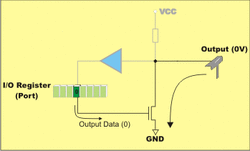
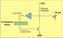
Input/Output (I/O) pin
Figure above illustrates a simplified schematic of all circuits within the microcontroler connected to one of its pins. It refers to all the pins except those of the P0 port which do not have pull-up resistors built-in.
Figure above illustrates a simplified schematic of all circuits within the microcontroler connected to one of its pins. It refers to all the pins except those of the P0 port which do not have pull-up resistors built-in.
Output pin
A logic zero (0) is applied to a bit of the P register. The output FE transistor is turned on, thus connecting the appropriate pin to ground.
A logic zero (0) is applied to a bit of the P register. The output FE transistor is turned on, thus connecting the appropriate pin to ground.
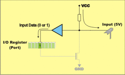
Input pin
A logic one (1) is applied to a bit of the P register. The output FE transistor is turned off and the appropriate pin remains connected to the power supply voltage over a pull-up resistor of high resistance.
A logic one (1) is applied to a bit of the P register. The output FE transistor is turned off and the appropriate pin remains connected to the power supply voltage over a pull-up resistor of high resistance.
Memory Organization
The 8051 has two types of memory and these are Program Memory and Data Memory. Program Memory (ROM) is used to permanently save the program being executed, while Data Memory (RAM) is used for temporarily storing data and intermediate results created and used during the operation of the microcontroller. Depending on the model in use (we are still talking about the 8051 microcontroller family in general) at most a few Kb of ROM and 128 or 256 bytes of RAM is used. However…
All 8051 microcontrollers have a 16-bit addressing bus and are capable of addressing 64 kb memory. It is neither a mistake nor a big ambition of engineers who were working on basic core development. It is a matter of smart memory organization which makes these microcontrollers a real “programmers’ goody“.
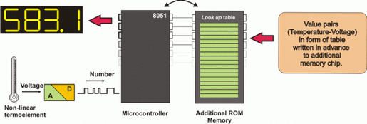
Program Memory The first models of the 8051 microcontroller family did not have internal program memory. It was added as an external separate chip. These models are recognizable by their label beginning with 803 (for example 8031 or 8032). All later models have a few Kbyte ROM embedded. Even though such an amount of memory is sufficient for writing most of the programs, there are situations when it is necessary to use additional memory as well. A typical example are so called lookup tables. They are used in cases when equations describing some processes are too complicated or when there is no time for solving them. In such cases all necessary estimates and approximates are executed in advance and the final results are put in the tables (similar to logarithmic tables).
